- 您现在的位置:买卖IC网 > Sheet目录995 > NCL30051LEDGEVB (ON Semiconductor)BOARD EVAL NCL30051 LED DRIVER
�� �
�
�NCL30051�
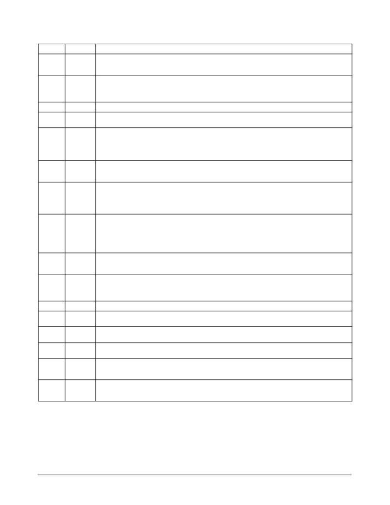
�Table� 1.� PIN� FUNCTION� DESCRIPTION�
�Pin�
�1�
�2�
�3�
�4�
�5�
�6�
�7�
�8�
�9�
�10�
�11�
�12�
�13�
�14�
�15�
�16�
�Name�
�HV�
�OSC�
�GND�
�VREF�
�PFB�
�PCS�
�PZCD�
�PControl�
�PCT�
�VCC�
�PGND�
�PDRV�
�HDRVlo�
�HVS�
�HDRVhi�
�HBoost�
�Description�
�This� is� the� input� of� the� high� voltage� startup� regulator� and� connects� directly� to� the� bulk� voltage.� A� constant� cur-�
�rent� source� supplies� current� from� this� pin� to� the� V� CC� capacitor,� eliminating� the� need� for� an� external� startup� res-�
�istor.� The� charge� current� is� 7.5� mA� (typical).�
�A� capacitor� on� this� pin� adjusts� the� frequency� of� the� internal� oscillator.� The� oscillator� sets� the� frequency� of� the�
�half� ?� bridge� controller.� Each� half� ?� bridge� switch� operates� at� half� the� oscillator� frequency.� The� OSC� pin� also�
�serves� as� a� disable� input� for� the� half� ?� bridge� stage.� The� half� ?� bridge� stage� is� disabled� by� pulling� down� this� pin�
�below� its� disable� threshold,� V� HB(DIS)� ,� typically� 1.955� V.�
�Analog� ground.�
�Reference� voltage.� The� capacitor� on� this� pin� decouples� the� internal� reference.� A� 0.1� m� F� capacitor� needs� to� be�
�connected� between� this� pin� and� ground.�
�PFC� voltage� feedback� input.� Connect� to� PFC� output� using� a� resistive� divider� network.� The� voltage� on� this� pin� is�
�compared� to� a� 2.5� V� reference� (typical)� to� regulate� the� PFC� output� voltage.� The� voltage� on� this� pin� is� also� used�
�to� detect� PFC� undervoltage� and� overvoltage� conditions.� In� the� typical� intended� application,� the� PFB� pin� voltage�
�will� set� an� upper� bound� on� the� PFC� output� voltage,� while� the� actual� PFC� voltage� control� will� be� exercised� by� a�
�control� signal� generated� on� the� secondary� side� to� provide� accurate� LED� current/voltage� control.�
�PFC� regulator� current� sense� input.� A� voltage� ramp� proportional� to� the� PFC� switch� current� is� applied� to� this� pin.�
�The� current� sense� threshold,� V� PCS(ILIM)� ,� is� typically� 0.84� V.� A� 110� ns� (typical)� leading� edge� blanking� circuit� filters�
�the� current� sense� signal� at� the� start� of� each� cycle.�
�PFC� inductor� zero� current� detector.� The� inductor� current� is� monitored� using� an� auxiliary� winding� on� the� PFC�
�inductor.� The� PFC� drive� signal� is� enabled� during� a� high� to� low� transition� on� the� PZCD� pin.� A� series� resistor� limits�
�the� current� into� the� PZCD� pin.� The� watchdog� timer� is� disabled� while� the� PZCD� voltage� is� above� the� ZCD� arming�
�threshold,� V� ZCD(high)� .� It� is� re� ?� enabled� once� the� voltage� drops� below� the� ZCD� trigger� threshold,� V� ZCD(low)� .� This�
�feature� can� be� used� to� disable� PFC� drive� pulses.�
�PFC� control� voltage.� This� pin� connects� to� the� output� of� the� PFC� error� amplifier.� The� error� amplifier� is� a� transcon-�
�ductance� amplifier.� A� compensation� network� between� this� pin� and� grounds� sets� the� PFC� loop� bandwidth.� The�
�PFC� control� voltage� is� compared� to� a� level� shifted� version� of� V� PCT� to� control� the� PFC� duty� ratio.� In� the� typical�
�intended� application,� the� PControl� voltage� will� be� controlled� by� a� secondary� side� control� signal� through� an� opto-�
�coupler.� The� optocoupler� signal� is� diode� ORed� to� the� internally� generated� PControl� signal� and� the� lower� of� the�
�two� signals� dictates� the� PFC� on-time.�
�PFC� on� time� control� capacitor.� A� 270� m� A� (typical)� current� source� charges� a� capacitor� connected� between� this�
�pin� and� ground.� Once� the� level� shifted� PCT� voltage� reaches� V� PControl� ,� the� PFC� drive� signal� is� disabled� and� the�
�PCT� capacitor� is� discharged.�
�Positive� input� supply.� This� pin� connects� to� an� external� capacitor� for� energy� storage.� An� internal� current� source�
�supplies� current� from� HV� to� this� pin.� Once� the� V� CC� voltage� reaches� V� CC(on)� (15.3� V� typical),� the� current� source�
�turns� off� and� the� controller� is� enabled.� The� current� source� turns� on� once� V� CC� falls� to� V� CC(off)� (9.3� V� typical).�
�During� normal� operation,� power� is� supplied� to� the� IC� via� this� pin� by� means� of� an� auxiliary� winding.�
�Ground� connection� for� PDRV� and� HDRVlo.� Tie� to� the� power� stage� return� with� a� short� trace.�
�PFC� switch� gate� drive� control� signal.� The� source� and� sink� drive� capability� is� limited� to� 60� W� and� 15� W� (typical),�
�respectively.� A� discrete� driver� may� be� needed� to� drive� the� external� MOSFET.�
�Half� ?� bridge� low� side� switch� gate� drive� control� signal.� The� source� and� sink� drive� capability� is� limited� to� 75� W� and�
�15� W� (typical),� respectively.� A� discrete� driver� may� be� needed� to� drive� the� half� bridge� switch.�
�Half� ?� bridge� high� side� driver� source� connection.� This� pin� connects� directly� to� the� bridge� terminal� and� can� float� up�
�to� 600� V.�
�Half� ?� bridge� high� side� switch� gate� drive� control� signal.� The� source� and� sink� drive� capability� is� limited� to� 75� W� and�
�15� W� (typical),� respectively.� The� supply� terminals� of� the� high� side� driver� connect� to� the� HBoost� and� HVS� pins.� A�
�discrete� driver� may� be� needed� to� drive� the� half� bridge� switch.�
�Supply� voltage� of� the� high� side� gate� driver.� A� charge� pump� generates� a� bootstrap� voltage� floating� on� top� of� the�
�HVS� voltage.� A� diode� between� the� VCC� and� HBoost� pins� provides� a� charge� path.� The� bootstrap� voltage� is� V� CC�
�minus� a� diode� drop.�
�http://onsemi.com�
�3�
�发布紧急采购,3分钟左右您将得到回复。
相关PDF资料
NCL30100ASLDGEVB
BOARD DEMO SGL LAYER PWM DIM LED
NCL30105GEVB
BOARD EVAL 80V 350 FOR LED DRV
NCP1013LEDGEVB
BOARD EVAL 5W UNIV LED DRIVER
NCP1028LEDGEVB
EVAL BOARD FOR NCP1028LEDG
NCP1216AFORWGEVB
BOARD EVAL NCP1216A 35W
NCP1351LEDGEVB
EVAL BOARD FOR NCP1351LEDG
NCP3065BBGEVB
BOARD EVAL NCP3065 MR16 BOOST
NCP3066SCBCKGEVB
EVAL BOARD FOR NCP3066SCBCKG
相关代理商/技术参数
NCL30080
制造商:ONSEMI 制造商全称:ON Semiconductor 功能描述:Quasi-Resonant Primary Side Current-Mode Side Current-Mode
NCL30080_13
制造商:ONSEMI 制造商全称:ON Semiconductor 功能描述:Quasi-Resonant Primary Side Current-Mode Controller for LED Lighting
NCL30080A
制造商:ONSEMI 制造商全称:ON Semiconductor 功能描述:Quasi-Resonant Primary Side Current-Mode Controller for LED Lighting
NCL30080ASNT1G
功能描述:LED照明驱动器 Quasi-Res I-Mode Cntlr
RoHS:否 制造商:STMicroelectronics 输入电压:11.5 V to 23 V 工作频率: 最大电源电流:1.7 mA 输出电流: 最大工作温度: 安装风格:SMD/SMT 封装 / 箱体:SO-16N
NCL30080B
制造商:ONSEMI 制造商全称:ON Semiconductor 功能描述:Quasi-Resonant Primary Side Current-Mode Controller for LED Lighting
NCL30080BSNT1G
制造商:ON Semiconductor 功能描述:PRIMARY SIDE CC FOR LED L - Tape and Reel
NCL30081
制造商:ONSEMI 制造商全称:ON Semiconductor 功能描述:Dimmable Quasi-Resonant Primary Side Current-Mode Controller for LED Lighting
NCL30081_13
制造商:ONSEMI 制造商全称:ON Semiconductor 功能描述:Dimmable Quasi-Resonant Primary Side Current-Mode Controller for LED Lighting